
In March, we travelled to Taiwan and Hong Kong for a 10-day trip. In Taiwan, we had meetings with 12 companies in their respective head offices. In Hong Kong, we participated in the 7th Jefferies Asia Forum, a large investor conference which connected over 180 Asian companies, 50 industry experts and 1,500 institutional investors. Over these 10 intense days, we held meetings with 22 companies. The list largely covered the tech sector focusing on semiconductor packaging and testing, IC design, components and equipment providers, clean room manufacturers and assembly: MPI corporation, Material Analysis, WinWay Technologies, Acter Group, C-Sun Manufacturing, RealTek Semiconductor Corporation, Global Unichip Corp, Zhen Ding Technology, ASE Technology, Quanta Computer, Elite Materials and Mediatek. In Hong Kong, we met 10 Asian companies such as Korean Memory maker SK Hynix, Indonesian telecom operator Telkom Indonesia, Indian bank AU Small Finance and Chinese companies such as internet players Baidu and JD.com, software provider Kingdee International Software, jewelry maker Chow Tai Fook, Education provider New Oriental Education, stock exchange platform Hong Stock Exchange and HK based REIT Link.
In Taipei, I also visited the TSMC Museum of Innovation which showcased the company’s technological leadership and unmatched manufacturing scale. In the evening, I took a stroll in Taipei’ famous night markets: where Jensen Huang (Nvidia CEO) has achieved celebrity status among local shop keepers, with photographs of his visits proudly displayed at food stalls, an illustration of how central AI has become to Taiwan.
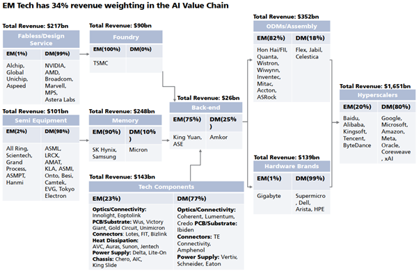
In March 2024, when we last visited Taiwanese companies in Taiwan, our focus centered on one single conviction: how artificial intelligence (AI) would reshape the global economy and TSMC fabricating high performance computing (HPC) chips designed by Nvidia, AMD and Broadcom would be critical enabler. Two years later, the thesis has gained significant traction, the top 4 hyper-scalers (Google, Amazon, Microsoft & Meta) have grown their AI capex from $200bn in 2024 to $620bn in 2025. During our time in Hong Kong, concerns were raised whether US AI capex has peaked. Jefferies Global strategist outlined three principal risks: hyper-scalers’ shareholders starting to question the ROIC of AI spending, constraints on power generation in USA leading to delays in data center build out and rising default swap spreads on Oracle and Core Weave (tier-2 hyper-scalers). Though on the ground in Taipei, the picture was strikingly different. Every company we met in the AI supply chain, packaging providers to equipment providers to chip designers, the message was clear ‘Demand for high-performance chips is accelerating, supply remains structurally constrained, and the production complexity required to meet that demand is only increasing’. We attribute the confidence in the supply chain to TSMC own signaling. The company raised its capex plan by 30-40% to $52-56bn in 2026, and approximately 20% to be allocated towards back-end infrastructure. A larger back-end allocation reflects the bottleneck shifting from front end fabrication to packaging of HPC chips. The advanced nodes of TSMC (2 & 3 nm) currently run at utilization rate of 100% and 120% in 4Q26. The advanced packaging capacity CoWoS is already being sold out and is being increased from 70,000 wafers per month (4Q25) to 170,000 wafers per month (4Q27). Even at this extended capacity, industry experts indicated that demand is likely to be 15-20% higher than supply. Against this backdrop, we would not be surprised to see TSMC announcing further capex to $65-70bn in 2027.
The packaging bottleneck is not simply a capacity story; it is also witnessing a technological transition. As HPC chips designed by Nvidia, AMD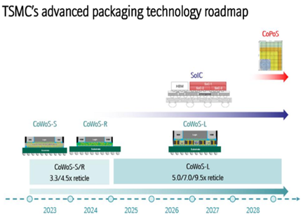 and Broadcom grow in complexity, the packaging processes required to interconnect them are evolving rapidly. TSMC is staging a migration across three generations in advanced packaging: Chip on Wafer on Substrate (CoWoS) to System on Integrated Chip (SoIC) to Chip on Panel on Substrate (CoPoS). While the capex intensity rises sharply as these technology shifts happen. Capex per 10K wafers: CoWoS ~$1.2-1.3bn, SoIC $2-2.3bn and CoPoS $1.7-1.9bn. Along with the technology migration, TSMC is aiming to develop the domestic supply chain by focusing on outsourcing. Industry experts indicated a goal to increase share of Taiwanese suppliers from 10% to 30% by 2028, a structural tailwind for domestic companies we visited. Each firm we met was building a specific, niche capability within the supply chain rather than competing head-on, which gives us confidence in the ecosystem ability to absorb this growth without competitive intensity rising. Our thesis remains contingent on sustained hyper-scalers AI capex, any meaningful reversal in that spending would put this outlook under pressure.
Macro focus:
Taiwan macro backdrop clearly reflects the AI boom. Real GDP grew by 12.7% yoy, driven by exports which rose by 38% yoy, reflecting stronger than expected dema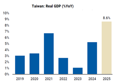 nd in AI driven semiconductor and ITrelated shipments. Domestic demand showed improvement, as real private consumption grew by 3.4% yoy supported by services spending through information & communication, entertainment, transport and outbound tourism. In 2025, Taiwan GDP growth was at a 10-year high of 8.6% way higher than potential growth rate of mid 3%. Meanwhile, February 2026 inflation picked up to a 10- month high of 1.8%, driven by pressure from energy supply. Taiwan sources 80% of its oil and 33% of its gas requirements from Middle East, which will need monitoring given the Iran conflict. Current storage stands at 100 days for oil and 11 days for LNG.
Company focus: ASE Holdings (Sales: $23bn - Market Capitalization: $50bn)
 Founded in 1984, by brothers Jason and Richard Chang as ASE Technology, the company vision was simple: to manage the unglamorous and technically demanding work of chips packaging and testing for the semiconductor industry. The company focused on Assembly, Testing & Materials (ATM). It has built capabilities in wire bonding, molding and final testing for DiP and SoIC packages for US and Japanese customers focusing on PC’s and Gaming consoles. As the smartphone revolution gained space in early 2000s, ASE Technology changed their trajectory by entering the electronic manufacutring services (EMS), by focusing on smaller, thinner and faster packages. In 2004, the company rolled out the System in Package (SiP) technology which gave them the ability to bundle multiple integrated chips into a single package. The technology won them a marquee customer Apple. In 2010, the company started developing 2.5D packaging solutions, a decade before the AI boom. In 2019, the company went through a major transformation. ASE technology merged with Silicon Precision Industries (SPIL) creating ASE Holdings to become one of the largest OSAT (Outsourced Semiconductor Assembly and Testing) player in the world with a combined market share of ~25% (as of 2025). The merger with SPIL led to scale, improvement in gross margins (16% in 2019 to 18% in 2025), reduction in competitive environment and a new customer: TSMC, who had a long collaboration with SPIL. In 2023, TSMC made a pivotal decision to outsource the back-end process of CoWoS, specifically the Wafer on Substrate (WoS) to ASE holdings, recognising their capabilites in advanced packaging. This marked the beginning of LEAP (Leading Advanced Packaging) business. In 2025, the company, generated sales of $1.6bn (13% of ATM sales). ASE Holdings continues to expand its capabilities as they roll out FoCoS (Fan Out Chip on Sustrate) for new customers such as AMD and AWS. Interestingly, the company is in discussion with TSMC for its CoPoS solutions, showcasing the strategic partnership between both companies. Separately, the company is seeing opportunity to grow its AI testing business from chip probing solutions to Final testing, as their testing equipment enters qualification stage with customers. We believe, the fundamental business transformation in LEAP and testing, can enable ASE Holdings to expand their LEAP sales to ~$6bn in 2027 (31% of ATM sales). A higher LEAP sales mix will carry structurally better margins, which should drive meaningful margin expansion for the company. Over a 2-year period (2026-2028), we expect the company sales to grow by 18% and EPS by 36%. The stock trades at FY26 P/E of 24.4x. We have invested 4.5% of GemEquity and 6.6% of GemAsia in the company.
Company focus: MPI Corporation (Sales: $650M - Market Capitalization: $12bn)
 Founded in 1995, MPI Corporation is a precision technology company engaged in designing and manufacturing probe card testing solutions, LED production equipment and advanced semiconductor test equipment. In the initial years, LED equipment business was the primary revenue driver. MPI supplied testing equipment that sorted and validated LED output prior to shipment, a stable cash generative business that the management used to fund R&D investment and build manufacturing capacities. This laid the foundation for MPI strategic pivot into the probe card business, which has grown to define the company. Probe card is a precision interface that presses thousands of tiny metallic needles simultaneously onto the electrical contact points of chips. Despite costing less than 1% of a chip’s total production cost, probe cards play an important role in influencing yield rates, which make them crucial in the supply chain. MPI corporation is one of the world’s top 5 probe card suppliers with a global market share of 8%. Over the years, MPI has built strong know-how and has ~800 customers. Notably, MPI can keep a 20% pricing premium to local Taiwanese suppliers and remain competitive with global peers, as they offer highly customized solutions to their customers. MPI offers 3 probe card solutions: Cantilever Probe card (CPC), which serves low to mid end chips (mainly consumer electronics), Vertical Probe card (VPC) and MEMS (Micro electromechanical systems) which serve higher end chips such as CPU/GPU and ASIC. Marquee CSP customers such as Broadcom, Marvell and Nvidia contribute 30% of overall sales. Complimenting the probe card division, MPI offers a suite of equipment solutions that perform reliability and durability checks at the wafer level. The three product lines are: Advanced Semi Testing (upon acquiring Celdon systems in 2021), Thermal equipment and Photonic automation used to produce LED. The first 2 contribute 90% of the equipment revenues and MPI enjoys a 30-40% market share in both categories. In 2025, the sales contribution from Probe card business was ~75% and from Equipment business ~25%. Interestingly, MPI has seen its gross margin expand from 42% in 2021 to 56% in 2026, driven by shift towards high margin VPC products along with insourcing of key components. Over the next 2 years, sales CAGR 2026-2028e is expected to grow by 46% and EPS by 65%. The stock trades at a high 2026 PER of 65X. We would be happy to get in at a lower valuation.
Rishabh Chudgar
Fund Manager - Gemway Assets